Hermetic. Ubiquitous. Guard. Zero.
SEALED PACKAGE · ONE MODULE ACROSS PLATFORMS · KEYS AND PQC KERNELS · ZERO STATE WHEN DE-ENERGIZED
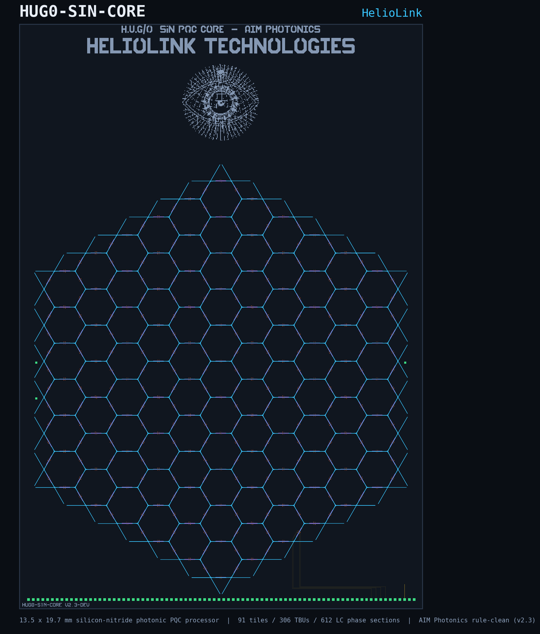
The die is a hexagonal mesh of silicon-nitride waveguides. Each side of each hexagon carries a tunable basic unit — a Mach-Zehnder interferometer with a liquid-crystal phase section in each arm, 612 sections across 306 TBUs. Setting a TBU's two phases sets the 2×2 unitary transformation light experiences on that edge; three TBUs meet at every Y-junction node, and 91 tiles of them make the mesh.
Program the phases along a path and the mesh performs matrix arithmetic as the light propagates. That matters for cryptography because the number-theoretic-transform butterfly — the operation that dominates ML-KEM and ML-DSA, the NIST lattice standards — is exactly a cascade of 2×2 operations. The mesh is the butterfly, laid out in waveguides.
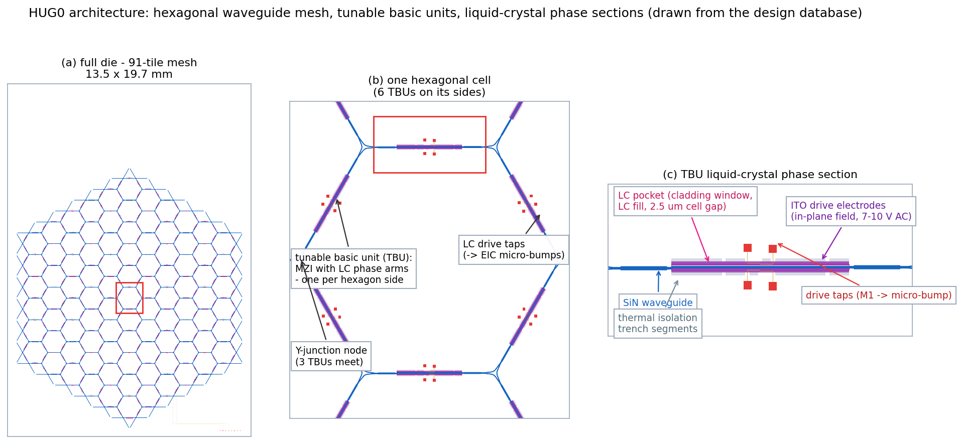
Die → cell → phase section, drawn from the design database. Red boxes mark the zoom path.
The usual way to tune a photonic mesh is a resistive heater on every phase arm. It works, but each section burns continuous power and leaks heat into its neighbors — costs that scale with all 612 sections. H.U.G.0 instead opens a window in the cladding over each arm and fills it with liquid crystal: a 2.5 µm cell gap over the SiN core, E7 as the baseline fill with MLC-2140 as the alternate, aligned by a polyimide layer.
ITO electrodes apply an in-plane AC field at 7–10 V. The field reorients the liquid-crystal director over the waveguide, changing the effective index — a pure phase shift, driven by field rather than current, with thermal-isolation trenches segmenting what little heat remains. The stack sits on a 300 mm SOI wafer.
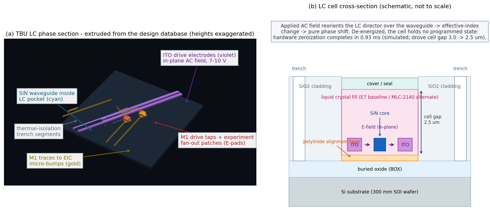
The phase section as drawn, and the cell cross-section (schematic, not to scale).
A liquid-crystal cell holds its state only while the field holds it. Cut power and the director relaxes: the phase program — the configured circuit itself — ceases to exist. In simulation, full hardware zeroization completes in 0.93 ms; that result is what drove the cell gap from 3.0 down to 2.5 µm.
For a module whose job is guarding keys, this inverts the usual engineering problem. Conventional secure hardware works hard to erase state under attack; here, persistence would take effort. A de-energized die is designed to carry no programmed state to read. That is the Zero in the name.
The 0.93 ms figure is simulated. Validating it on first silicon is an explicit goal of the characterization plan below.
First-article testing is designed around a deliberately conventional electrical chain: an FR-4 carrier board, ENEPIG bond fingers, 1-mil gold wirebonds onto 90 µm die pads, reaching eight liquid-crystal channels in two mesh sections — two cascaded 2×2 unitaries, one complete NTT butterfly, programmable end to end. Full-mesh drive of all 612 sections arrives later, with an electronic IC flip-chipped onto 1,224 micro-bumps.
Optically, the die presents 72 edge couplers on its east and west facets, each a spot-size converter tapering an 8 µm fiber mode down to the 0.9 µm waveguide, designed at roughly 0.75 dB per facet. On the probe station the interface is free-space butt-coupling from a lensed fiber; the permanent package uses AIM's fiber-array attach process — SMF-28, actively aligned on loopback structures.
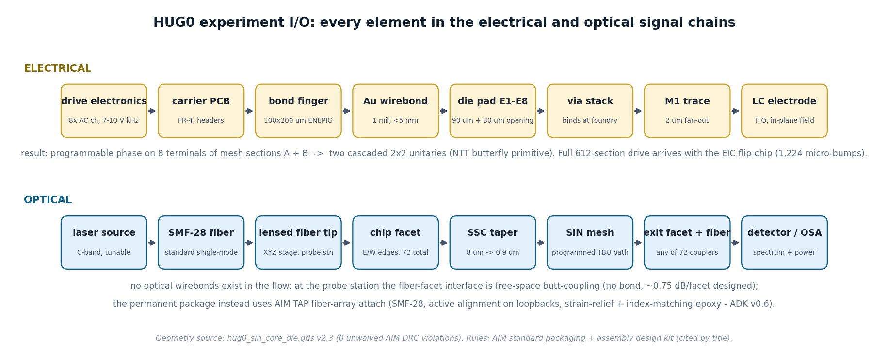
Design database v2.3, rule-clean against the AIM Photonics process design kit with zero unwaived DRC violations. Packaging and assembly follow AIM's standard packaging and assembly design kit.
The die carries its own test plan: the eight-channel wirebond experiment, optical loopback structures for alignment, and fiducials for assembly. No optical wirebonds exist anywhere in the flow — probe-station work is butt-coupled, and the package interface is the fiber array.
What exists today: a complete, rule-clean design database and a characterization plan built into the die. What does not exist yet: fabricated silicon, measured optical or electrical data, or any certification. The zeroization time is simulated; the coupling losses are design values. Fabrication through the AIM Photonics ecosystem is the next step, and we will publish measured results when there are measured results.
How this fits the company: the die is the hardware expression of our research program — photonic acceleration of the NIST post-quantum kernels — and the compute half of the H.U.G.0 module concept, alongside the NASA-licensed optical link technology.
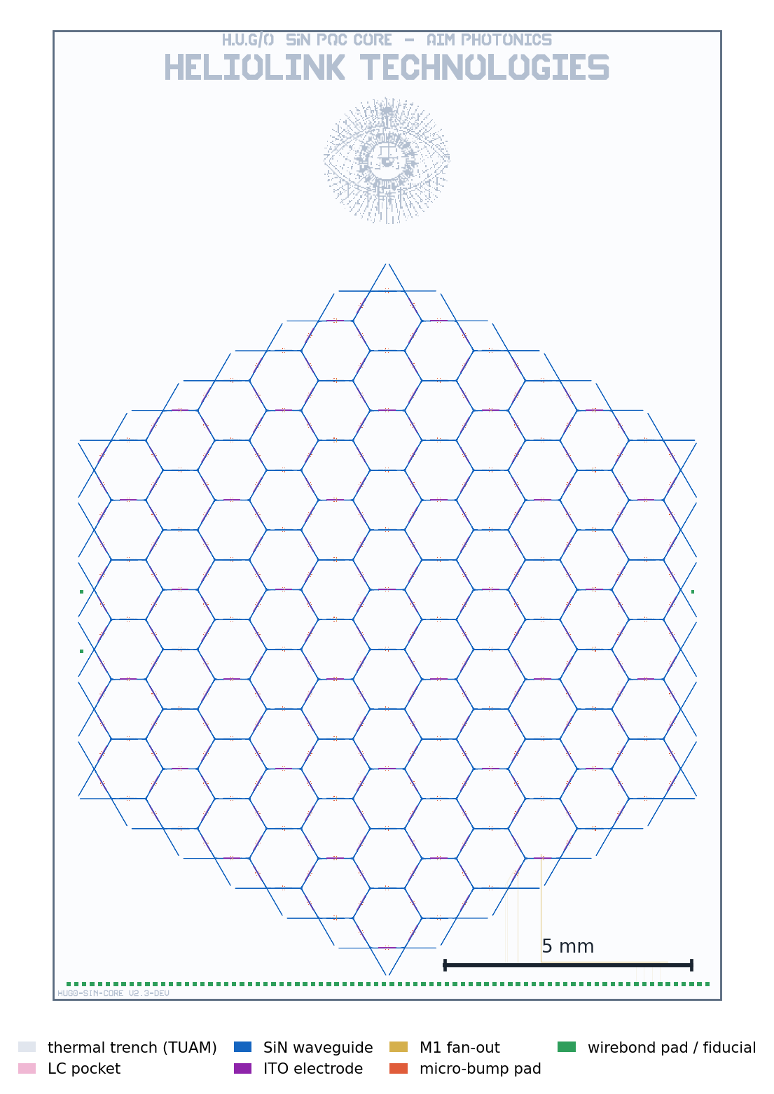
The die as drawn: every layer in the legend, 5 mm scale bar.
Our white paper sets out the case this die is built on: NIST's standardized PQC schemes cost 30–100× more processing than classical cryptography on constrained devices, and photonic offloading plus validated quantum entropy is our research response. Sources cited inline; claims scoped the same way this page scopes them.
Read the white paper (PDF)HelioLink Technologies white paper · v2.0 · December 2025